The
box in which all the computer components are housed, next to your
monitor or below your table, is often referred to as a "CPU". Really
though, the actual Central Processing Unit is just a small chip inside
the computer. Everything else in the box is connected to it to help it
process instructions and provide results.
The CPU is
the core of any computer. It's what's also known as the processor, and is a
lot smaller than most people imagine. The shiny metal that you see is
only a heatsink, called the "integrated heat spreader", and is mounted
on top of the actual chip. It transfers heat away from the CPU to ensure
stable operation (silicon transistors have certain temperature ranges
in which they perform optimally, and would get damaged without proper
cooling).
The CPU is made up of a control unit and an arithmetic
and logic unit (ALU). The control unit controls how incoming data is
processed by the CPU, and hands the processed result to its destination.
This
input data comes from the computer's memory. Present day computers are
designed around the stored program architecture, also known as the Von
Neumann Architecture. What this means (in the sense of method, plan or
algorithm) is that data must be loaded from memory, and the result
processed by the ALU must be stored into memory as well.
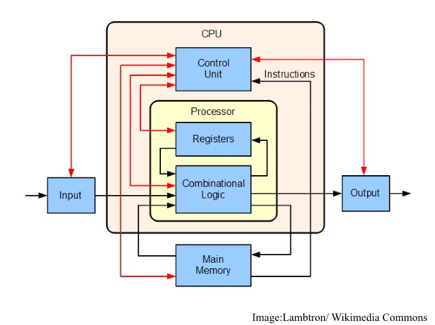
This
exchange happens via a memory interface, under the directive of the
control unit. This interface tracks two things: the memory location from
which the data is read/ written, and the data transfer process itself.
So
how does the ALU know what to do with the data? Well, we'll have to
split the program code (residing in memory) into two parts: instructions
and data. Basically, the CU expects the first thing read from the
memory to be an instruction operation code, or simply "opcode" which
describes the physical resources needed on the ALU, and the amount of
data expected to follow. Thus, the first few bytes will be the
instruction op code, and the next few bytes will be the data to be
processed. Depending upon what specific instructions the ALU receives,
it can do different things with the data.
The final pieces of the
puzzle are registers, which are temporary spaces for data (or
instructions) inside the CPU itself, which are used to feed the ALU
faster than program code can be retrieved from memory.
Instruction set architectures
That
was a simplified blueprint of a CPU, which only represents modern-day
CPUs at a very high level. Today's CPUs contain billions of transistors,
with millions of units of logic circuits operating over a billion times
a second.
Processor architectures (both the actual physical
layout and the abstracted logical layout) have evolved and expanded
significantly over the years. They now implement sophisticated
pipelining, branching, threading, and a whole host of other techniques
to improve performance by ensuring that instructions are ready when
needed, and that the results of operations executed simultaneously are
assembled in the right order.
There are two fundamental types of
instruction set architectures (ISAs): RISC and CISC. RISC stands for
Reduced Instruction Set Computing and CISC stands for Complex Instruction
Set Computing. The basic difference between these two lies in the way
instructions are formed. RISC implements only a small set of simple
instructions, whereas CISC uses more complicated instructions that are
broken down internally into simpler commands before being processed.
The
apparent advantage of RISC is that a complicated instruction takes less
time when interpreted as a set of smaller instructions. On the other
hand, CISC handles the intricacies of algorithms rather than requiring
programmers to do so, making it easier to write assembly code (the "low-level" language used to talk to the microprocessor almost
directly).
Intel's x86 is an example of CISC architecture, while
ARM's ARMv7 is a RISC design. Debate about the "best" way to do things
in CPU design has raged on for decades now, and while RISC vs. CISC used
to matter a lot in the 80s and 90s, there's little reason now to
consider either better.
Either way, ISA refers to a broad set of
instructions, methods, timing information (more on this later),
algorithms, etc. which work together so that implementations of the ISA
are compatible with each other. While the ISA is a broad blueprint,
specific physical implementations can, and usually do, vary. That means
AMD can engineer its processors differently from Intel's as long as they
conform to the base x86 ISA.
When the limits of 32-bit x86 CPUs became apparent, Intel chose to develop an all-new architecture (called Itanium) whereas AMD worked on extensions to x86. Itanium failed to gain traction due to a lack of backward compatibility, and so AMD64 became the default industry standard. As a result, Intel had to cross-license AMD's 64-bit extensions, and so x86-64 is a common standard. The conformity ensures that software can
run without any problem across different chips.
Companies that
have licensed an ISA can do different things to improve performance and
reduce power consumption. The can also add additional fixed function
logic or otherwise extend functionality using their own ISA extensions.
Each different physical
implementation of an ISA is called a microarchitecture, and this
differentiation is often the basis of processor codenames. Haswell,
Broadwell, Nehalem, Silvermont, Bulldozer, Steamroller, etc. are
codenames that apply to families of processors based on a single
microarchitecture. These are usually not the brand names exposed to the
public. For example, Intel's Haswell processors are sold as 4th
Generation Core Processors. Core i3, Core i5 and Core i7 are brands
which are used to differentiate capabilities within families.
In
Part 2, we talk about 64-bit computing, CPU cores, clock speeds, and
the things that make some CPUs more powerful than others.

 Microsoft Says Next-Gen Xbox Will Run on AMD Chip, Not Be 'Locked to a Single Store'18 June 2025


