

-
 Huawei, Qualcomm Announce Multi-Year Patent Licensing Agreement Covering 5G, AI and More5 October 2026
 -
Huawei FreeBuds 7 Launched With ANC and Up to 33-Hour Battery Life: Price, Features8 September 2026
-
Huawei Pura X View Launched With 200-Megapixel Camera, 7,000mAh Battery: Price, Specifications8 September 2026
-
Huawei Mate XT 2 Ultimate Design Launched With Kirin 9050 Pro Chipset: Price, Specifications7 September 2026
-
Huawei Watch 6 and Watch 6 Pro Announced at IFA 2026; Watch GT 7 and GT 7 Pro Tag Along3 September 2026
- Home
- Laptops
- Laptops News
- Huawei Wants to Surpass Moore’s Law Constraints With Its New Scaling System
Huawei Wants to Surpass Moore’s Law Constraints With Its New Scaling System
Huawei’s Tau Scaling Law introduces a time-based scaling framework to improve system performance and transistor density.
Written by Akash Dutta, Edited by Ketan Pratap | Updated: 25 May 2026 17:23 IST
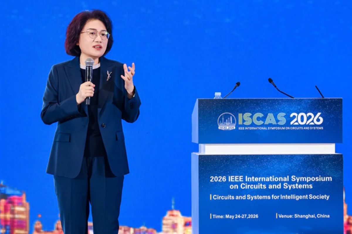
Photo Credit: Huawei
Huawei plans to combine hardware and software to achieve higher performance in chips
Click Here to Add Gadgets360 As A Trusted Source

Advertisement
The semiconductor industry is quickly reaching an inflection point. Last year, Samsung began mass production of the initial 2nm node for the Exynos 2600 chipsets. Other players, including TSMC, Qualcomm, MediaTek, and Intel, have also reached significant milestones when it comes to the technology. So far, Moore's Law is intact (at least in spirit). But beyond this, adhering to the law will become nearly impossible due to physical restraints and technology bottlenecks. As an alternative, Huawei has presented a new system dubbed the Tau Scaling Law.
The Problem With Moore's Law
Coined by Intel Co-Founder Gordon Moore in 1965, Moore's Law is an empirical observation that the number of transistors on a microchip doubles roughly every two years while the cost of a computer halves. Ever since, it has governed the exponential growth of computational power and the affordability of these devices. But six years later, most experts and technologists have acknowledged that Moore's Law is dead.
It has been dead for some time now. The reality is that even with the 2nm process technology, Moore's Law is being kept alive in spirit (some might call it cheating). While the transistor density has doubled, the number of actual physical transistors on the wafer has only increased by 15 to 20 percent. The reason behind this is that the transistors do not really measure two nanometres.
A silicon atom is about 0.2nm wide, which means 2nm is only 10 atoms across. At this size, quantum physics causes electrons to lean uncontrollably. So, the current 2nm process technology is only a marketing nomenclature to signify that the chips perform as if their sizes were scaled down to that size. In reality, companies are using new packaging architectures and stacking strategies, such as System-on-Integrated-Chips, to increase performance.
Enter Huawei's Tau Scaling Law
He Tingbo, President of the Semiconductor Business Department at Huawei, delivered a keynote speech at the 2026 IEEE International Symposium on Circuits and Systems (ISCAS) on Monday. During the speech, she presented the tau Scaling Law, a new guiding principle for the future development of the semiconductor industry.
In a newsroom post, Huawei said the law proposes “replacing geometric scaling with time scaling as a new guiding principle for the evolution of both semiconductors and electronic systems.” It also claimed that “innovative technologies such as LogicFolding can be used to continuously compress signal propagation delay and steadily improve transistor density.”
The Tau Scaling Law proposes using time as a scaling mechanism by reusing physical hardware elements over processing or execution time within the same piece of silicon. Put simply, instead of asking, “How many physical transistors can be fit on this chip?”, it asks, “How can we reuse the existing transistors multiple times within a single execution cycle?”
So, while in Moore's Law, the only way to get 1,000 logic steps is by building 1,000 physical logic gates on the chip, with Tau's law, it can be reached by building a smaller set of highly flexible gates and dynamically “folding” them to process those steps sequentially in time.
And to answer the “how,” Huawei said innovative core technologies, such as LogicFolding and other architectures that use a multi-level software-hardware combination across devices, circuits, chips, and systems, can help. So, instead of breaking down the physical boundaries of traditional circuit layout, Huawei suggests using a software system to dynamically alter how many gates can be executed in a nanosecond.
Interestingly, this is not just an exercise in theoretical physics either. During the keynote, the executive revealed that by 2031, Huawei will design chipsets based on the Tau Scaling Law that feature a transistor density that is equivalent to a 1.4nm process chip.
Comments
Get your daily dose of tech news, reviews, and insights, in under 80 characters on Gadgets 360 Turbo. Connect with fellow tech lovers on our Forum. Follow us on X, Facebook, WhatsApp, Threads and Google News for instant updates. Catch all the action on our YouTube channel.
Related Stories





Advertisement
Follow Us




-
![[Sponsored]: CP PLUS CarKam CP-F89B: 4K Dashcam With Rear Camera, GPS & Emergency Recording](https://www.gadgets360.com/static/desktop/images/spacer.png)
04:37
[Sponsored]: CP PLUS CarKam CP-F89B: 4K Dashcam With Rear Camera, GPS & Emergency Recording -
04:23
[Partner Content] Your Phone Can Do WAY More Than You Think | OPPO ColorOS 16 -
01:59
Samsung Galaxy Z Fold8 Ultra: Unfold the Ultra Night -
03:24
Apple Pay Launches In India: Supported Devices, Cards And Payments Explained -
00:21
[Sponsored] Samsung Galaxy Z Fold8, Fold8 Ultra
-
Amazon Great Indian Festival Sale 2026: ₹15,999 से शुरू स्मार्टफोन डील्स
-
घर की दीवार बनेगी 120 इंच की सिनेमा स्क्रीन! Lumio Arc 7 (2026) हुआ लॉन्च
-
Amazon Great Indian Festival Sale 2026: ₹18 हजार सस्ता मिलेगा iPhone 16!
-
Oppo Find X10 Pro Max जल्द होगा भारत में लॉन्च, MediaTek Dimensity 9600 Pro चिपसेट
-
Lenovo ने लॉन्च किया AI फीचर्स वाला ThinkBook 14x लैपटॉप, आपकी पसंद के मिलेंगे फीचर्स
Advertisement
Popular on Gadgets
- Samsung Galaxy S26 Ultra
- Motorola Razr Fold
- ChatGPT
- OPPO Find N6
- Mobiles Under Rs. 40,000
- Vivo X300 Ultra
- Asus Zenbook S14
- iQOO 15
- Vivo X300 Pro
- Lenovo Yoga Slim 7i Aura Edition
- iQOO 15R
- Vivo X Fold 5
- Sony PlayStation 5
- HP OmniPad 12
- OnePlus Nord CE 6 Lite
- OnePlus Pad 4
- OPPO F33 Pro 5G
- Cryptocurrency
- HP OmniBook Ultra 14 (2026)
- iPhone 17
- Eureka Forbes AP 355 Room Air Purifier
- Latest Mobile Phones
- Compare Phones
Latest Gadgets
- Vivo Y32 (2026)
- Infinix Smart 20 HD
- Vivo V80
- Vivo S2 FE
- Vivo Y600K Turbo
- Realme P4s Lite
- Vivo S60t
- OPPO F35 5G
- Lenovo ThinkBook 14x
- Dell 14 Plus 2-in-1 (AMD Ryzen AI 7 350, 2025)
- Samsung Galaxy Tab S12+
- Samsung Galaxy Tab S12 Ultra
- Amazfit T-Rex Dual Solar
- OPPO Watch S2
- Toshiba 65-Inch 4K Ultra HD Smart Mini LED QLED TV (65Z670SP)
- Haier M70 Mini LED 65-inch
- Acer Predator Atlas 8
- Asus ROG Ally
- Blue Star 1.5 Ton 5 Star Inverter Split AC (IE518ZNURS)
- Blue Star 2 Ton 3 Star Inverter Window AC (WIE324L)

- About Us
- Sitemaps
- Feedback
- Archives
- Contact Us
- RSS
- Advertise
- Career
- Privacy Policy
- Ethics
- Editorial Policy
- Terms & Conditions
- Complaint Redressal
Download Our Apps
Available in Hindi
© Copyright Red Pixels Ventures Limited 2026. All rights reserved.